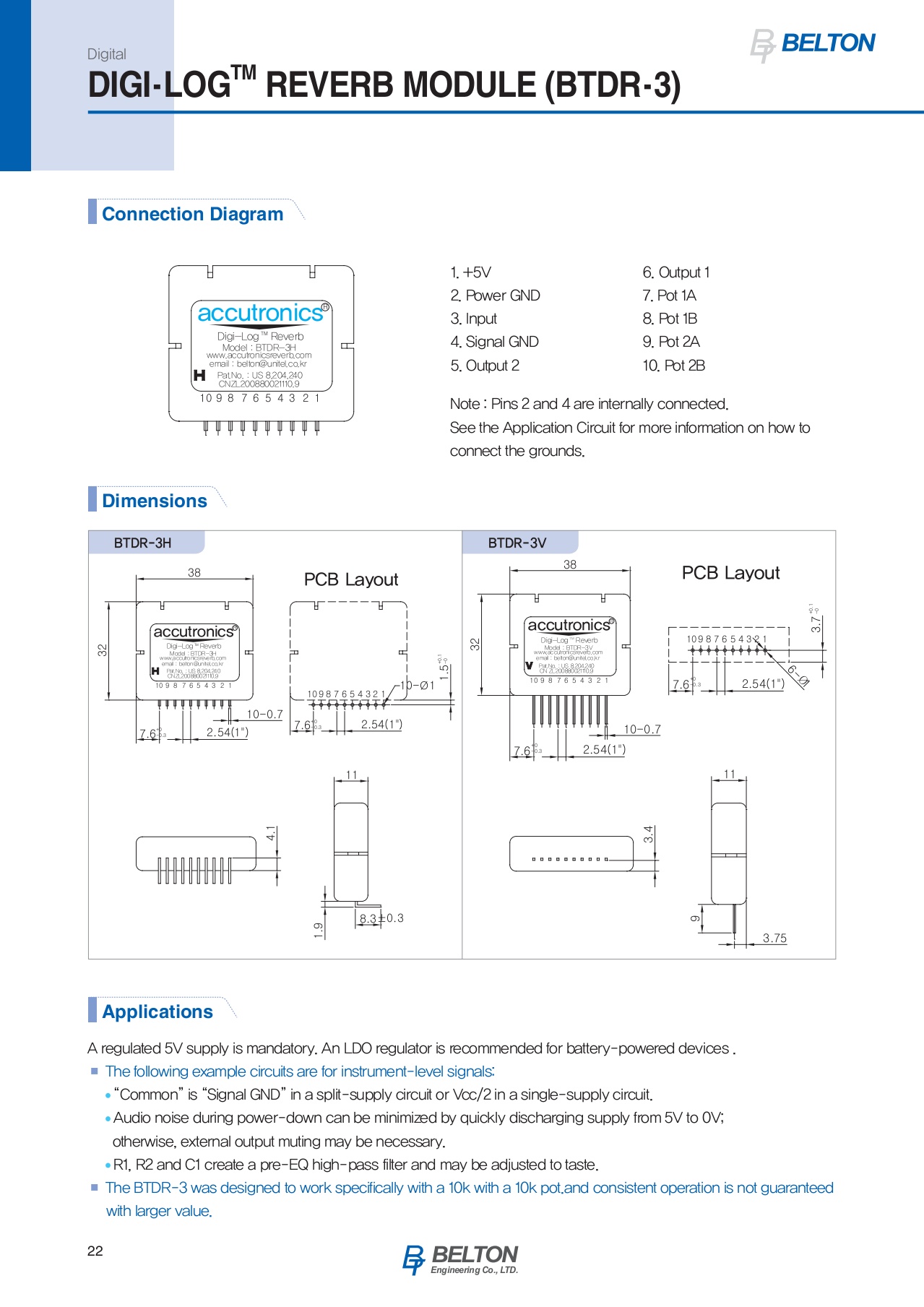

Digital TM DIGI- LOG REVERB MODULE (BTDR- 3) Connection Diagram 1. +5V 6. Output 1 2. Power GND 7. Pot 1A 3. Input 8. Pot 1B 4. Signal GND 9. Pot 2A 5. Output 2 10. Pot 2B Note : Pins 2 and 4 are internally connected. See the Application Circuit for more information on how to connect the grounds. Dimensions BTDR- 3H BTDR- 3V Ø Applications A regulated 5V supply is mandatory. An LDO regulator is recommended for battery- powered devices . ■ The following example circuits are for instrument- level signals: “Common” is “Signal GND” in a split-supply circuit or Vcc/2 in a single-supply circuit. Audio noise during power- down can be minimized by quickly discharging supply from 5V to 0V; otherwise, external output muting may be necessary. R1, R2 and C1 create a pre- EQ high- pass filter and may be adjusted to taste. ■ The BTDR-3 was designed to work specifically with a 10k with a 10k pot.and consistent operation is not guaranteed with larger value. 22 Engineering Co., LTD.

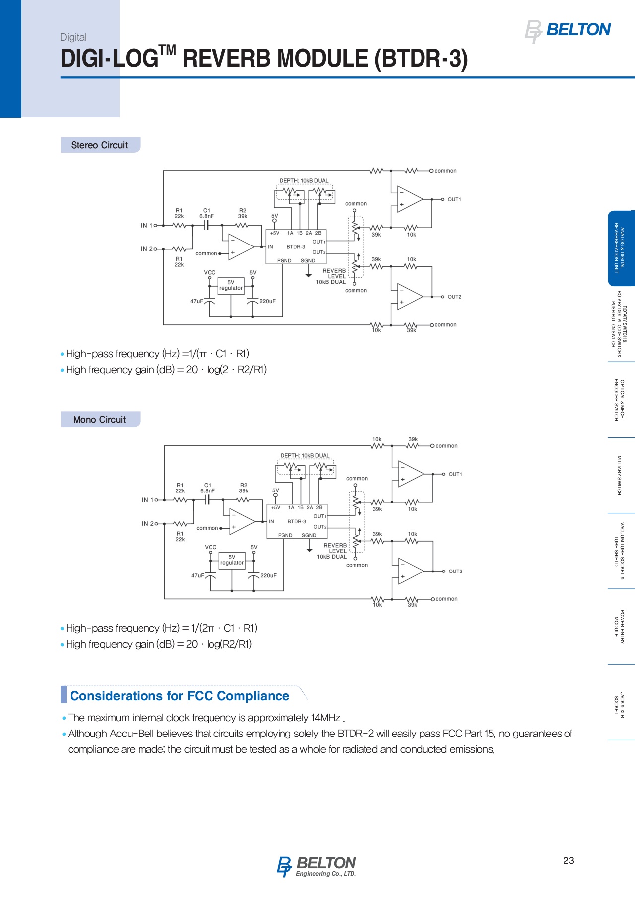
Digital TM DIGI- LOG REVERB MODULE (BTDR- 3) Stereo Circuit R E R A E V A V N E N E A R A R L B L B O E O E G R G R A & A & T T D I D I O O I I G N G N I I T U T U A N A N L I L T I T R O T A P R U Y S R H D O I T B G A I U T R T A Y T L O C S N O W I S D T W E C I S H T W & C H I T C H High- pass frequency (Hz) =1/(πㆍC1ㆍR1) & High frequency gain (dB) = 20ㆍlog(2ㆍR2/R1) E O N C P T O I D C E A R L & S W M I E T C C H Mono Circuit H . M I L I T A R Y S W I T C H V A C U T U U M B T E U S B H E I S E L O D C K E T & P O M W O E D R High- pass frequency (Hz) = 1/(2πㆍC1ㆍR1) U E L N E T R Y High frequency gain (dB) = 20ㆍlog(R2/R1) J S A Considerations for FCC Compliance O C K C K & E X T L The maximum internal clock frequency is approximately 14MHz . R Although Accu - Bell believes that circuits employing solely the BTDR- 2 will easily pass FCC Part 15, no guarantees of compliance are made; the circuit must be tested as a whole for radiated and conducted emissions. 23 Engineering Co., LTD.