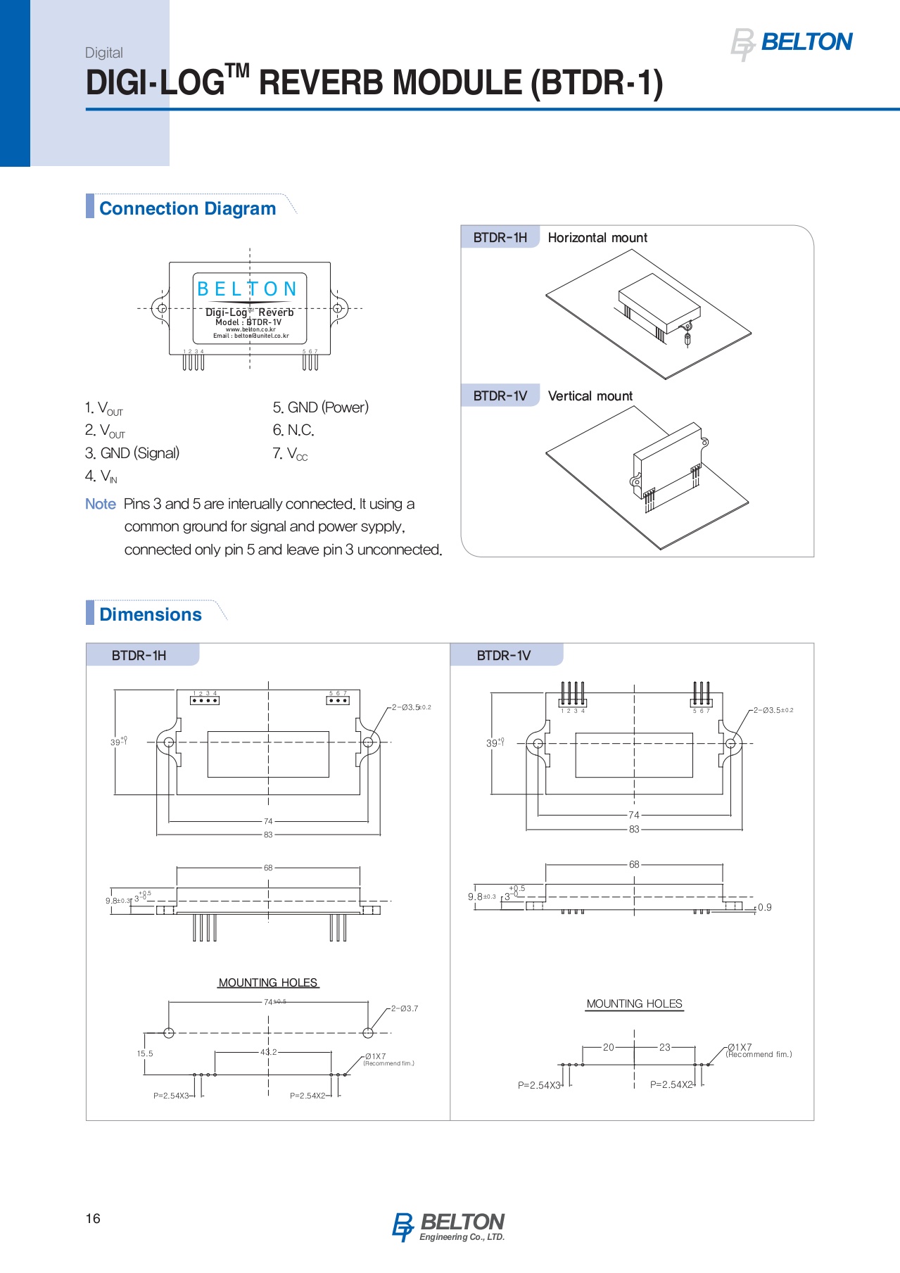

Digital TM DIGI- LOG REVERB MODULE (BTDR- 1) Connection Diagram BTDR- 1H Horizontal mount B E L T O N TM Digi-Log Reverb Model : BTDR-1V www.belton.co.kr Email : belton@unitel.co.kr 1 2 3 4 5 6 7 OUT 1.V 5.GND(Power) BTDR- 1V Vertical mount OUT 2.V 6.N.C. 1. VOUT 5. GND (Power) CC 3.GND(Signal) 7.V 2. VOUT IN 6. N.C. 4.V 3. GND (Signal) 7. VCC 4. VIN Note Pins 3 and 5 are interually connected. It using a common ground for signal and power sypply, connected only pin 5 and leave pin 3 unconnected. Dimensions BTDR- 1H BTDR- 1V 16 Engineering Co., LTD.

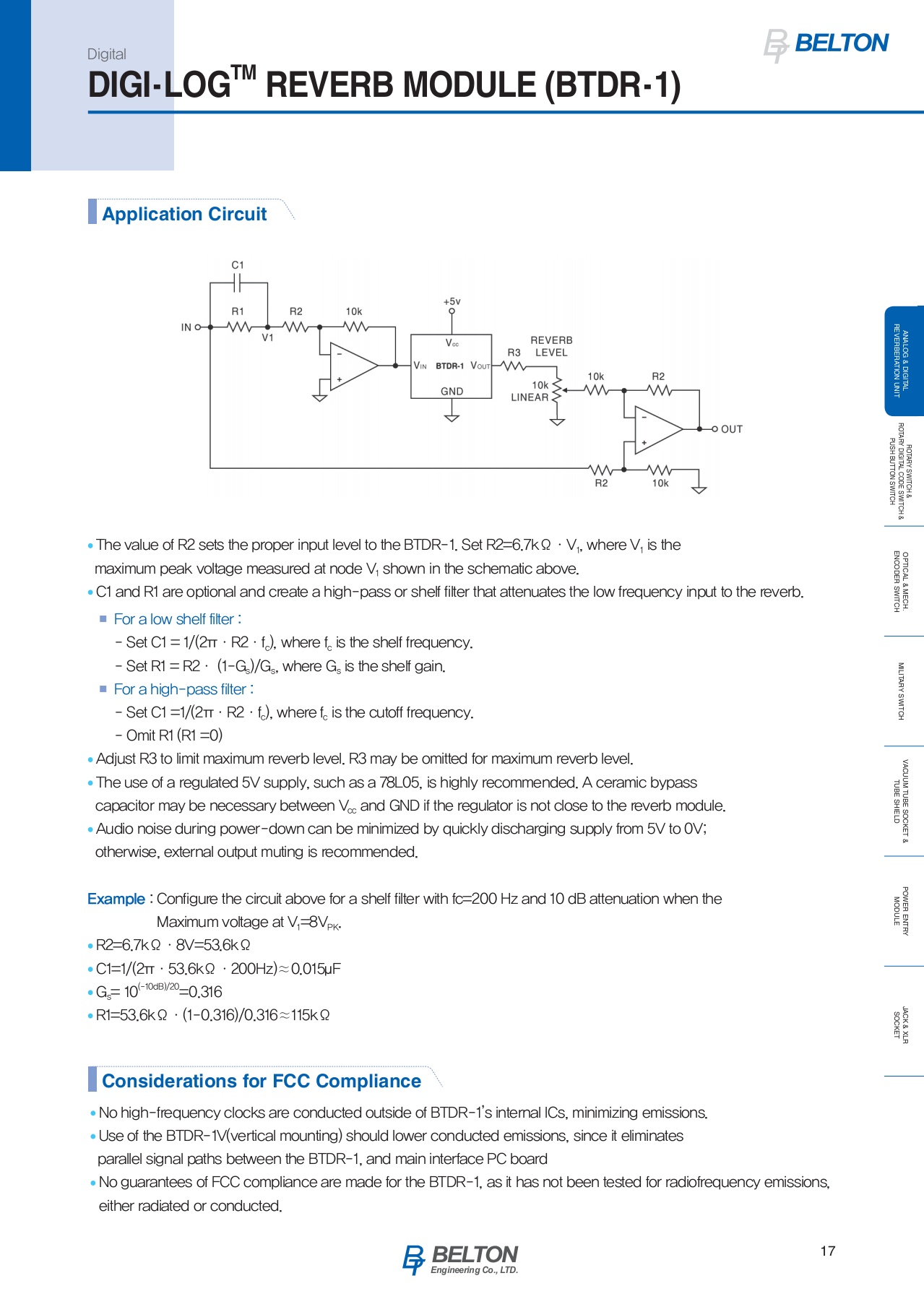
Digital TM DIGI- LOG REVERB MODULE (BTDR- 1) Application Circuit R E R A E V A V N E N E A R A R L B L B O E O E G R G R A & A & T T D I D I O O I I G N G N I I T U T U A N A N L I L T I T R O T A P R U Y S R H D O I T B G A I U T R T A Y T L O C S N O W I S D T W E C I S H T W & C H I T C H & The value of R2 sets the proper input level to the BTDR- 1. Set R2=6.7kΩㆍV , where V is the E O 1 1 N C P T O I maximum peak voltage measured at node V shown in the schematic above. D C 1 E A R L & S W M C1 and R1 are optional and create a high- pass or shelf filter that attenuates the low frequency input to the reverb. I E T C C H H . ■ For a low shelf filter : - Set C1 = 1/(2πㆍR2ㆍf ), where f is the shelf frequency. c c M I - Set R1 = R2ㆍ (1- G )/G , where G is the shelf gain. L s s s I T A R Y ■ For a high- pass filter : S W I T C - Set C1 =1/(2πㆍR2ㆍf ), where f is the cutoff frequency. H c c - Omit R1 (R1 =0) Adjust R3 to limit maximum reverb level. R3 may be omitted for maximum reverb level. V A C U T U The use of a regulated 5V supply, such as a 78L05, is highly recommended. A ceramic bypass U M B T E U S B H E capacitor may be necessary between V and GND if the regulator is not close to the reverb module. I S cc E L O D C K E Audio noise during power- down can be minimized by quickly discharging supply from 5V to 0V; T & otherwise, external output muting is recommended. P O M W Example : Configure the circuit above for a shelf filter with fc=200 Hz and 10 dB attenuation when the O E D R U E L N Maximum voltage at V =8V . E T 1 PK R Y R2=6.7kΩㆍ8V=53.6kΩ C1=1/(2πㆍ53.6kΩㆍ200Hz)≈0.015μF G = 10(- 10dB)/20=0.316 s J S A O C R1=53.6kΩㆍ(1- 0.316)/0.316≈115kΩ K C K & E X T L R Considerations for FCC Compliance No high-frequency clocks are conducted outside of BTDR- 1’s internal lCs, minimizing emissions. Use of the BTDR- 1V(vertical mounting) should lower conducted emissions, since it eliminates parallel signal paths between the BTDR- 1, and main interface PC board No guarantees of FCC compliance are made for the BTDR- 1, as it has not been tested for radiofrequency emissions, either radiated or conducted. 17 Engineering Co., LTD.